Electrical Concepts
Tricky but Easy Electrical Engineering!

Travelling Wave on Transmission Line
Travelling wave on transmission line is the voltage / current waves which propagate from the source end to the load end during the transient condition. These waves travel along the line with the velocity equal to velocity of light if line losses are neglected. But practically there always exists some line loss and hence these waves propagate along the line with velocity somewhat lower than the velocity of light.
Concept of Travelling Wave
We know that short transmission line and medium transmission line are studied by their equivalent T or π model . But these models are only useful to study and analyze the steady state response of the line. In case where we are interested in the study of transient behavior, these models are not useful as the line parameters are actually not lumped rather they are non-uniformly distributed over the entire length of the line. For transient analysis , it is very important to consider the line parameters like shunt capacitance and inductance to be distributed and hence their effect must be considered.
Let us consider a lossless transmission line. Let L and C be the inductance and capacitance per unit length of the line.

The above transmission line can be represented by its equivalent circuit having L and C distributed over the whole line as shown below.

When the switch S is closed, the voltage at the load end does not appear immediately at the load end. As soon as the Switch S is closed, inductance L1 acts as open circuit and capacitance C1 acts as short circuit. Therefore as far as the capacitor C1 is not charged to some value, the charging of C2 through L2 is not possible. This means that charging of C2 through L2 will take some finite time. Similar reasoning applies to the other successive sections. Thus we see that whenever switch S is closed, there is a gradual voltage build up from the source end to the load end over the transmission line. This gradual voltage build up can be thought of due to a voltage wave travelling from one end to the other and the gradual charging of capacitor through inductor is due to current wave.
Let us understand this voltage and current wave in different wave by taking one analogy. Replace the switch S by water valve and each section of inductor and capacitor by a water tank as shown below.

When the water valve is opened, tank A will first fill up to the level of interconnection between the tanks due to flow of water from the valve. This water flow is the flow of current through the inductor L. And the tank level is nothing but the voltage developed across the shunt capacitor C. Once the tank A is filled up, tank B will start filling and when it is also filled up to the level, tank C will start to fill. This means that the filling of tank C will be complete after some finite time and not immediately. Thus the flow of water from tank A to tank C can be assumed as a wave propagating from tank A to tank C. Similarly, the tank levels can also be thought of a wave moving from tank A to tank C. Hope you understood the phenomenon of travelling wave on transmission line by this simple analogy.
Till now, we understood that there are current and voltage wave travelling over the line. Now we want to get the relationship between these two waves.
Relationship between Voltage and Current Wave:
Let the voltage wave and current wave travels a distance x in time t. Therefore the inductance and capacitance of line up to distance x will be Lx and Cx respectively. Let this wave travels a distance dx in time dt.
Since line is assumed to be lossless, whatever is the value of voltage wave and current wave at the beginning, the same will be at any time t. This means that, the magnitude of voltage and current wave at time t will be V and I respectively.
Hence the stored charge in shunt capacitance Q = VCx
and the flux in the series inductance Ø = ILx
But I = dQ/dt
= CVdx/dt
But dx/dt = velocity of travelling wave = ν (say)
Therefore, I = CVν …….(1)
The voltage developed across the shunt capacitance,
⇒V = ILν ……….(2)
Dividing equation (1) and (2), we get
V / I = IL / CV
(V/I) 2 = L/C
V/I = √(L/C)
The above expression is the ratio of voltage and current having the dimension of impedance. Therefore it is called Surge Impedance. Note that Surge Impedance is the square root of ratio of series inductance L per unit length of line and shunt capacitance C per unit length of line. This simply means that this value will remain constant for a given transmission line. This value will not change due to change in length of line. The value of surge impedance for a typical transmission line is around 400 Ohm and that for a cable is around 40 ohm. Notice that the value of surge impedance for cable is less than that of transmission line. This is due to the higher value of capacitance of cable compared to the transmission line.
Velocity of Travelling Wave:
To get velocity of travelling wave, multiply (1) and (2) as below.
VI = (CVν) x (LIν)
ν = √(1/LC) ……..(3)
The above expression is the velocity of travelling wave. Since L and C are per unit values, the velocity of travelling wave is constant. For overhead line the values of L and C are given as
L = 2×10 -7 ln(d/r) Henry / m
C = 2πε / ln (d/r)
From (3), the velocity of travelling wave for overhead line
ν = 1 / [{2×10 -7 ln(d/r)}{ 2πε / ln (d/r)}] 1/2
= 1/[4πεx10 -7 ] 1/2
The permittivity of air, ε = (1/36π) x 10 -9
ν = 1 / [4πx(1/36π) x 10 -9 x10 -7 ] 1/2
= 3 x10 8 m/sec.
From the above expression, we can have following conclusions:
The velocity of travelling wave for a lossless line is equal to the speed of light.
Since the cable core is surrounded by insulations and sheath , its relative permittivity ε r >1 and hence ε = ε 0 ε r > ε 0 (permittivity of air). Therefore the speed of travelling wave on cable is less than that of transmission line.
3 thoughts on “Travelling Wave on Transmission Line”
Great Content! Really Insightful for the students. Didn’t Know That “The velocity of travelling wave for a lossless line is equal to the speed of light”
very well explained. thanks for sharing.
Leave a Comment Cancel reply
Notify me when new comments are added.
Travelling Waves on Transmission Lines:
Any disturbance on a Travelling Waves on Transmission Lines or system such as sudden opening or closing of line, a short circuit or a fault results in the development of overvoltages or overcurrents at that point. This disturbance propagates as a travelling wave to the ends of the line or to a termination, such as, a sub-station.
Usually these Travelling Waves on Transmission Lines are high frequency disturbances and travel as waves. They may be reflected, transmitted, attenuated or distorted during propagation until the energy is absorbed. Long transmission lines are to be considered as electrical networks with distributed electrical elements.
In Fig. 8.14, a typical two-wire transmission line is shown along with the distributed electrical elements, R, L, C and G.

The propagation of any Travelling Waves on Transmission Lines, say a voltage wave can be analysed by considering an elemental length of the line dx. The voltage drop in the positive x-direction in the elemental length dx due to the inductance and resistance is
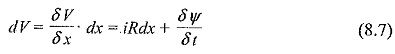
Here, δψ is the change of flux linkages and is equal to i.L.dx, where i the current through the line.

The shunt current through the leakage conductance (G) and capacitance (C) is
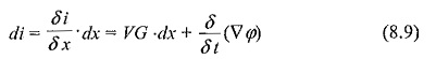
Here, ∇φ is the change in electrostatic field flux and is equal to VC.dx, where V is the potential at the point x.

Hence, the above equations can be written as
Taking Laplace transform with respect to the time variable t, the equations can be put in the operation form as

Eliminating i and V from above equations and differentiating w.r.t. x, we get

where the product YZ = γ 2 = RG + (RC + LG)s + LCs 2 .
The above two equations are called W ave Equations or Telegraphic Equations . The solutions for the above equations can be written in the form:
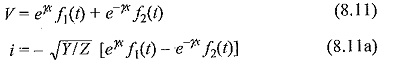
where f 1 (t) and f 2 (t) are any arbitrary functions that satisfy the boundary conditions. The operator γ is simplified as

Y(s) is called the surge admittance, the reciprocal of which
Related Posts:
Voltage drop on load and regulation, high voltage test on insulators, insulation coordination of substation, paschen breakdown, solid dielectric materials, electric field stress, peak reading voltmeter circuit, cascade transformer connection, electrostatic voltmeters, townsend current growth equation.
Travelling Wave
Definition: Travelling wave is a temporary wave that creates a disturbance and moves along the transmission line at a constant speed. Such type of wave occurs for a short duration (for a few microseconds) but cause a much disturbance in the line. The transient wave is set up in the transmission line mainly due to switching, faults and lightning.
The travelling wave plays a major role in knowing the voltages and currents at all the points in the power system. These waves also help in designing the insulators, protective equipment, the insulation of the terminal equipment, and overall insulation coordination.
Specifications of Travelling Wave
The travelling wave can be represented mathematically in a number of ways. It is most commonly represents in the form of infinite rectangular or step wave. A travelling wave is characterised by four specifications as illustrated in the figure below.

Crest – it is the maximum aptitude of the wave, and it is expressed in kV or kA.
Front – It is the portion of the wave before the crest and is expressed in time from the beginning of the wave to the crest value in milliseconds or µs.
Tail – The tail of the wave is the portion beyond the crest. It is expressed in time from the beginning of the wave to the point where the wave has reduced to 50% of its value at its crest.
Polarity – Polarity of the crest voltage and value. A positive wave of 500 kV crest 1 µs front and 25 µs tail will be presented as +500/1.0/25.0.
Surge is a type of travelling wave which is caused because of the movement of charges along the conductor. The surge generates because of a sudden vary steep rise in voltage (the steep front) followed by a gradual decay in voltage (the surge tail). These surges reach the terminal apparatus such as cable boxes, transformers or switchgear, and may damage them if they are not properly protected.
Travelling Wave on Transmission Line
The transmission line is a distributed parameter circuit and its support the wave of voltage and current. A circuit with distributed parameter has a finite velocity of electromagnetic field propagation. The switching and lightning operation on such types of circuit do not occur simultaneously at all points of the circuit but spread out in the form of travelling waves and surges.
When a transmission line is suddenly connected to a voltage source by the closing of a switch the whole of the line in not energised at once, i.e., the voltage does not appear instantaneously at the other end. This is due to the presence of distributed constants (inductance and capacitance in a loss-free line).
Considered a long transmission line having a distributed parameter inductance (L) and capacitance (C). The long transmission line is divided into small section shown in the figure below.The S is the switch used for closing or opening the surges for switching operation. When the switch is closed the L1 inductance act as an open circuit and C 1 act as a short circuit. At the same instant, the voltage at the next section cannot be charged because the voltage across the capacitor C 1 is zero.

So unless the capacitor C 1 is charged to some value the charging of the capacitor C 2 through L 2 is not possible which will obviously take some time. The same argument applies to the third section, fourth section, and so on. The voltage at the section builds up gradually. This gradual build up of voltage over the transmission conductor can be regarded as though a voltage wave is travelling from one end to the other end and the gradual charging of the voltage is due to associate current wave.
The current wave, which is accompanied by voltage wave steps up a magnetic field in the surrounding space. At junctions and terminations, these waves undergo reflection and refraction. The network has a large line and junction the number of travelling waves initiated by a single incident wave and will increase at a considerable rate as the wave split and multiple reflections occurs. The total energy of the resultant wave cannot exceed the energy of the incident wave.
Related terms:
- Half Wave and Full Wave Rectifier
- Difference Between Electromagnetic Wave and Matter Wave
- Lap & Wave Winding
- Difference Between Lap & Wave Winding
- Full Wave Bridge Rectifier
2 thoughts on “Travelling Wave”
Thanks for ur kind information
Good explanation
Leave a Comment Cancel Reply
Your email address will not be published. Required fields are marked *
Save my name, email, and website in this browser for the next time I comment.

- school Campus Bookshelves
- menu_book Bookshelves
- perm_media Learning Objects
- login Login
- how_to_reg Request Instructor Account
- hub Instructor Commons
- Download Page (PDF)
- Download Full Book (PDF)
- Periodic Table
- Physics Constants
- Scientific Calculator
- Reference & Cite
- Tools expand_more
- Readability
selected template will load here
This action is not available.
2.3: The Terminated Lossless Line
- Last updated
- Save as PDF
- Page ID 41014

- Michael Steer
- North Carolina State University
Microwave engineers want to work with total voltage and current when possible and the art of design synthesis usually requires relating the total voltage and current world of a lumped element circuit to the traveling voltage world of transmission lines. This section develops the important abstractions that enable the total voltage and current view of the world to be used with transmission lines. The first step in this process is in Section 2.3.1 where total voltages and currents are related to forward- and backward-

Figure \(\PageIndex{1}\): A terminated transmission line.
traveling voltages and currents. Insight into traveling waves and reflections is presented in Section 2.3.2. Important abstractions are presented first for the input reflection coefficient of a terminated lossless line in Section 2.3.3 and then for the input impedance of the line in Section 2.3.4. The last section, Section 2.3.5, presents a view of the total voltage on the transmission line and describes the voltage standing wave concept.
2.3.1 Total Voltage and Current on the Line
Consider the terminated line shown in Figure \(\PageIndex{1}\)(a). Assume an incident or forward-traveling wave, with traveling voltage \(V_{0}^{+}e^{−\jmath\beta z}\) and current \(I_{0}^{+}e^{−\jmath\beta z}\) propagating toward the load \(Z_{L}\) at \(z = 0\). The characteristic impedance of the transmission line is the ratio of the voltage and current traveling waves so that
\[\label{eq:1}\frac{V_{0}^{+}(z)}{I_{0}^{+}(z)}=\frac{V_{0}^{+}e^{-\jmath\beta z}}{I_{0}^{+}e^{-\jmath\beta z}}=\frac{V_{0}^{+}(0)}{I_{0}^{+}(0)}=\frac{V_{0}^{+}}{I_{0}^{+}}=Z_{0} \]
The reflected wave has a similar relationship (but note the sign change):
\[\label{eq:2}\frac{V_{0}^{-}e^{\jmath\beta z}}{-I_{0}^{-}e^{\jmath\beta z}}=\frac{V_{0}^{-}}{-I_{0}^{-}}=Z_{0} \]
The load \(Z_{L}\) imposes an additional constraint on the relationship of the total voltage and current at \(z = 0\):
\[\label{eq:3}\frac{V_{L}}{I_{L}}=\frac{V(z=0)}{I(z=0)}=Z_{L} \]
When \(Z_{L}\neq Z_{0}\) there must be a reflected wave with appropriate amplitude to satisfy the above equations. Now the total voltage
\[\label{eq:4}V(z)=V_{0}^{+}e^{-\jmath\beta z}+V_{0}^{-}e^{\jmath\beta z} \]
and the total current, \(I(z)\), is related to the traveling current waves by
\[\label{eq:5}I(z)=\frac{V_{0}^{+}}{Z_{0}}e^{-\jmath\beta z}-\frac{V_{0}^{-}}{Z_{0}}e^{\jmath\beta z}=I_{0}^{+}e^{-\jmath\beta z}+I_{0}^{-}e^{\jmath\beta z} \]
Thus at the termination of the line \((z = 0)\),
\[\frac{V(0)}{I(0)}=Z_{L}=Z_{0}\frac{V_{0}^{+}+V_{0}^{-}}{V_{0}^{+}-V_{0}^{-}}\nonumber \]
This can be rearranged as the ratio of the reflected voltage to the incident voltage:
\[\frac{V_{0}^{-}}{V_{0}^{+}}=\frac{Z_{L}-Z_{0}}{Z_{L}+Z_{0}}\nonumber \]
This ratio is defined as the voltage reflection coefficient at the load,
\[\label{eq:6}\Gamma_{L}=\Gamma_{L}^{V}=\frac{V_{0}^{-}(0)}{V_{0}^{+}(0)}=\frac{V_{0}^{-}}{V_{0}^{+}}=\frac{Z_{L}-Z_{0}}{Z_{L}+Z_{0}} \]
That is, at the load
\[\label{eq:7}V_{0}^{-}=\Gamma_{L}V_{0}^{+} \]
The relationship of the traveling waves on the line can also be described using the transmission coefficient \(T\) (this is the capital Greek letter tau which looks the same as the English letter ‘T’.)
The voltage transmission coefficient from a port at position \(z\) to a port at position \(0\) is (for the transmission line)
\[\label{eq:8}T=T^{V}=\frac{V_{0}^{+}\text{ (at end of line)}}{V_{0}^{+}\text{ (at start of line)}}=\frac{V_{0}^{+}(0)}{V_{0}^{+}(z)}=\frac{V_{0}^{+}}{V_{0}^{+}e^{-\jmath\beta z}}=e^{\jmath\beta z} \]
The relationship in Equation \(\eqref{eq:6}\) can be rewritten so that the input load impedance can be obtained from the reflection coefficient:
\[\label{eq:9}Z_{L}=Z_{0}\frac{1+\Gamma^{V}}{1-\Gamma^{V}} \]
Similarly, the current reflection coefficient can be written as
\[\label{eq:10}\Gamma^{I}=\frac{I_{0}^{-}}{I_{0}^{+}}=\frac{-Z_{L}+Z_{0}}{Z_{L}+Z_{0}}=-\Gamma^{V} \]
The voltage reflection coefficient is used most of the time, so the reflection coefficient, \(\Gamma\), on its own refers to the voltage reflection coefficient, \(\Gamma^{V}=\Gamma\).
There are several special cases that are noteworthy. The most important of these is the case when there is no reflected wave and \(\Gamma=0\). To obtain \(\Gamma=0\), the value of load impedance, \(Z_{L}\), is equal to \(Z_{0}\), the characteristic impedance of the transmission line as seen in Equation \(\eqref{eq:6}\).
The total voltage and current waves on the line can be written as
\[\label{eq:11}V(z)=V_{0}^{+}[e^{-\jmath\beta z}+\Gamma e^{\jmath\beta z}] \]
\[\label{eq:12}I(z)=\frac{V_{0}^{+}}{Z_{0}}[e^{-\jmath\beta z}-\Gamma e^{\jmath\beta z}] \]
From Equations \(\eqref{eq:11}\) and \(\eqref{eq:12}\) it can be seen that the total voltage and current on the line consist of superpositions of incident and reflected waves.
Example \(\PageIndex{1}\): Forward- and Backward- Traveling Waves at an Open Circuit
A lossless transmission line is terminated in an open circuit. What is the relationship between the forward- and backward-traveling voltage waves at the end of the line?
At the end of the line the total current is zero, so that \(I^{+} + I^{−} = 0\) and so
\[\label{eq:13}I^{-}=-I^{+} \]
The forward- and backward traveling voltages and currents are related to the characteristic impedance by
\[\label{eq:14}Z_{0}=V^{+}/I^{+}=-V^{-}/I^{-} \]
Note the change in sign, as a result of the direction of propagation changing but the positive reference for current is in the same direction. Substituting for I− at the termination,
\[\label{eq:15}V^{+}=-V^{-}I^{+}/I^{-}=-V^{-}I^{+}/(-I^{+})=V^{-} \]
Thus the total voltage at the end of the line, \(V_{\text{TOTAL}}\), is \(V^{+} + V^{−} = 2V^{+}\). Note that the total voltage at the end of the line is twice the incident (forward-traveling) voltage.
Example \(\PageIndex{2}\): Current Reflection Coefficient
A load consists of a shunt connection of a capacitor of \(10\text{ pF}\) and a resistor of \(60\:\Omega\). The load terminates a lossless \(50\:\Omega\) transmission line. The operating frequency is \(5\text{ GHz}\).
- What is the impedance of the load?
- What is the normalized impedance of the load (normalized to \(Z_{0}\) of the line)?
- What is the reflection coefficient of the load?
- What is the current reflection coefficient of the load?
- \(C = 10\cdot 10^{−12}\text{ F};\: R = 60\:\Omega ;\: f = 5\cdot 10^{9}\text{ Hz};\: \omega = 2πf;\: Z_{0} = 50\:\Omega\) \[Z_{L} = R||C = (1/R + \jmath\omega C)^{−1} = 0.168 −\jmath 3.174\:\Omega\nonumber \]
- \(z_{L} = Z_{L}/Z_{0} = 3.368\cdot 10^{−3} −\jmath 0.063\).
- This is the voltage reflection coefficient. \(\Gamma_{L} = (z_{L} − 1)/(z_{L} + 1) = −0.985 −\jmath 0.126 = 0.993\angle 187.3^{\circ}\).
- \(\Gamma_{L}^{I} = −\Gamma_{L} = 0.985 +\jmath 0.126 = 0.993\angle (187.3 − 180)^{\circ} = 0.993\angle 7.3^{\circ}\).
2.3.2 Forward- and Backward-Traveling Pulses
Reflections at the end of a line produce a backward-traveling signal. Forward- and backward-traveling pulses are shown in Figure \(\PageIndex{2}\)(a) for the situation where the resistance at the end of the line is lower than the characteristic impedance of the line \((Z_{L} < Z_{0})\). The voltage source is a step voltage that is zero for time \(t < 0\). At time \(t = 0\), the step is applied to the line and it begins traveling down the line, as shown at time \(t = 1\). This voltage step moving from left to right is called the forward-traveling voltage wave.
At time \(t = 2\), the leading edge of the step reaches the load, and as the load has lower resistance than the characteristic impedance of the line, the total voltage across the load drops below the level of the forward-traveling voltage step. The reflected wave is called the backward-traveling wave and it must be negative, as it adds to the forward-traveling wave to yield the total voltage. Thus the voltage reflection coefficient, \(\Gamma\), is negative and the total voltage on the line, which is all that can be directly observed, drops. A reflected, smaller, and opposite step signal travels in the backward direction and adds to the forward-traveling step to produce the waveform shown at \(t = 3\). The impedance of the source matches the transmission line impedance so that the reflection at the source is zero. The signal on the line at time \(t = 4\), the time for round-trip propagation on the line, therefore remains at the lower value. The easiest way to remember the polarity of the reflected pulse is to consider the situation with a short-circuit at the load. Then the total voltage on the line at the load must be zero. The only way this can occur when a signal is incident is if the reflected signal is equal in magnitude but opposite in sign, in this case \(\Gamma = −1\). So whenever \(|Z_{L}| < |Z_{0}|\), the reflected pulse will tend to subtract from the incident pulse.
The opposite situation occurs when the resistance at the load is higher than the characteristic impedance of the line (Figure \(\PageIndex{2}\)(b)). In this case the reflected pulse has the same polarity as the incident signal. Again, to remember this, think of the open-circuited case. The voltage across the load doubles, as the reflected pulse has the same sign as well as magnitude as that of the incident signal, in this case \(\Gamma = +1\). This is required so that the total current is zero.
A more illustrative situation is shown in Figure \(\PageIndex{3}\), where a more

Figure \(\PageIndex{2}\): Reflection of a voltage pulse from a load: (a) when the resistance of the load, \(R_{L}\) is lower than the characteristic impedance of the line, \(Z_{0}\); and (b) when \(R_{L}\) is greater than \(Z_{0}\).

Figure \(\PageIndex{3}\): Reflection of a pulse on an interconnect showing forward- and backward-traveling pulses. \(Z_{L} > Z_{0}\).
complicated signal is incident on a load that has a resistance higher than that of the characteristic impedance of the line. The peaking of the voltage that results at the load is typically the design objective in many long digital interconnects, as less overall signal energy needs to be transmitted down the line, or equivalently a lower current drive capability of the source is required to achieve first incidence switching. This is at the price of having reflected signals on the interconnects, but these are dissipated through a combination of line loss and absorption of the reflected signal at the driver.
2.3.3 Input Reflection Coefficient of a Lossless Line
The reflection coefficient looking into a line varies with position along the line as the forward- and backward-traveling waves change in relative phase. Referring to Figure \(\PageIndex{4}\), at a distance \(\ell\) from the load (i.e., \(z = −\ell\)), the input

Figure \(\PageIndex{4}\): Terminated transmission line: (a) a transmission line terminated in a load impedance, \(Z_{L}\), with an input impedance of \(Z_{\text{in}}\); and (b) a transmission line with source impedance \(Z_{G}\) and load \(Z_{L}\).

Figure \(\PageIndex{5}\): The forward-traveling wave \(v^{+}(t, z) = |V^{+}| \cos(\omega t −\beta z) = |V^{+}| \cos(\omega t + \phi (z))\) and the backward-traveling wave \(v^{−}(t, z) = |V^{+}| \cos(\omega t +\beta z) = |V^{+}| \cos[\omega t + \phi (z)]\). The phase, \(\phi\), of the forward-traveling wave becomes increasingly negative along the line as \(z\) increases, and when reflected the phase \(\phi\) of the backward-traveling wave becomes increasingly negative as the wave moves away from the load (i.e. as \(z\) decreases).
reflection looking into a terminated lossless line is
\[\label{eq:16}\Gamma_{\text{in}}|_{z=-\ell}=\frac{V^{-}(z=-\ell)}{V^{+}(z=-\ell)}=\frac{V^{-}(z=0)e^{-\jmath\beta\ell}}{V^{+}(z=0)e^{+\jmath\beta\ell}}=\frac{V^{-}(z=0)}{V^{+}(z=0)}\frac{e^{-\jmath\beta\ell}}{e^{+\jmath\beta\ell}}=\Gamma_{L}e^{-\jmath 2\beta\ell} \]
Note that \(\Gamma_{\text{in}}\) has the same magnitude as \(\Gamma_{L}\) but rotates in the clockwise direction (becomes increasingly negative) at twice the rate of increase of the electrical length \(\beta\ell\).
It is important to graphical concepts introduced later that there be a full appreciation for the angle of \(\Gamma_{\text{in}}\) becoming increasingly negative at twice the rate at which the electrical length of the line increases. Figure \(\PageIndex{5}\) is a way of visualizing this. The transmission line here is \(\lambda/4\) long with an electrical length of \(90^{\circ}\) and is terminated in a load with reflection coefficient \(\Gamma_{L} = +1\). At position \(z = 0\) the forward-traveling voltage wave is \(v^{+}(t, 0) = |V^{+}| \cos(\omega t)\), and this then propagates down the line in the \(+z\) direction. The forward-traveling voltage at point \(z = \lambda /8\) at \(t = 0\) will be the same as the voltage at \(z = 0\) at a time one-eighth of a period in the past. The voltage at \(z =\lambda/8\) is \(v^{+}(t, \lambda/8) = |V^{+}| \cos(\omega t − 2π/8)\), i.e. there is a phase rotation of \(−45^{\circ}\). Then at \(z = \lambda /4\), \(v^{+}(t, \lambda/4) = |V^{+}| \cos(\omega t − 2π/4)\), i.e. at time \(t = 0\) there is a phase rotation of \(−90^{\circ}\) relative to \(v^{+}(0, 0)\), and this is the negative of the electrical length of the line. The voltage wave reflects at the load and becomes a backward-traveling wave. Here \(\Gamma_{L} = +1\) and so, at the load, the phase of the backward- and forward-traveling waves are the same. The backward-traveling wave continues to travel in the \(−z\) direction and its phase at \(t = 0\) becomes increasingly negative as \(z\) gets closer to the input of the line. The phase of the backward-traveling wave at \(z = 0\) is rotated \(−90^{\circ}\) with respect to the backward-traveling wave at the load, and has rotated \(−180^{\circ}\) relative to the forward-traveling wave at \(z = 0\). For a lossless line, in general, the angle of \(\Gamma_{\text{in}} = [\text{phase of }V^{−}(z = 0)\) relative to the phase of \(V^{+}(z = 0)] + (\text{the phase of }\Gamma_{L}) = −2(\text{electrical length of the line}) + (\text{the phase of }\Gamma_{L})\).
2.3.4 Input Impedance of a Lossless Line
The impedance looking into a lossless line varies with position, as the forward- and backward-traveling waves combine to yield position-dependent total voltage and current. At a distance \(\ell\) from the load (i.e., \(z = −\ell\)), the input impedance seen looking toward the load is
\[\label{eq:17}Z_{\text{in}}|_{z=-\ell}=\frac{V(z=-\ell)}{I(z=-\ell)}=Z_{0}\frac{1+|\Gamma|e^{\jmath(\Theta -2\beta\ell)}}{1-|\Gamma|e^{\jmath(\Theta-2\beta\ell)}}=Z_{0}\frac{1+\Gamma_{L}e^{\jmath(-2\beta\ell)}}{1-\Gamma_{L}e^{\jmath(-2\beta\ell)}} \]
Another form is obtained by substituting Equation \(\eqref{eq:6}\) in Equation \(\eqref{eq:17}\):
\[\begin{align}Z_{\text{in}}&=Z_{0}\frac{(Z_{L}+Z_{0})e^{\jmath\beta\ell}+(Z_{L}-Z_{0})e^{-\jmath\beta\ell}}{(Z_{L}+Z_{0})e^{\jmath\beta\ell}-(Z_{L}-Z_{0})e^{-\jmath\beta\ell}}=Z_{0}\frac{Z_{L}\cos(\beta\ell)+\jmath Z_{0}\cos(\beta\ell)}{Z_{0}\cos(\beta\ell)+\jmath Z_{L}\cos(\beta\ell)}\nonumber \\ \label{eq:18}&=Z_{0}\frac{Z_{L}+\jmath Z_{0}\tan\beta\ell}{Z_{0}+\jmath Z_{L}\tan\beta\ell}\end{align} \]
This is the lossless telegrapher’s equation . The electrical length, \(\beta\ell\), is in radians when used in calculations.
2.3.5 Standing Waves and Voltage Standing Wave Ratio
The total voltage on a terminated line is the sum of forward- and backward-traveling waves. This sum produces what is called a standing wave. Figure \(\PageIndex{6}\) shows the total and traveling waveforms on a line terminated in a reactance and evaluated at times equal to multiples of an eighth of a period. Here the traveling waves have the same amplitude indicating that the termination of the line is reactive, \(|\Gamma| = 1\). The interesting property here is that the total voltage appears as a standing wave with fixed points called nodes where the total voltage is always zero. This is more easily seen in Figure \(\PageIndex{7}\)(a), where the total voltage is overlaid for many times. If the termination has resistance, then the magnitude of the backward-traveling wave will be less than that of the forward-traveling wave and the overlaid total voltage is as shown in Figure \(\PageIndex{7}\)(b). This is still a standing wave, but the minima are now not zero. The envelope of this standing wave is shown in Figure \(\PageIndex{7}\)(c), where there is a maximum amplitude \(V_{\text{max}}\) and a minimum amplitude \(V_{\text{min}}\).
Now this situation will be examined mathematically to relate the standing wave to the reflection coefficient. If \(\Gamma=0\), then the magnitude of the total voltage on the line, \(|V(z)|\), is equal to \(|V_{0}^{+}|\) anywhere on the line. For this reason, such a line is said to be “flat.” If there is reflection the magnitude of the total voltage on the line is not constant (see Figure \(\PageIndex{7}\)(b)). Thus from Equations \(\eqref{eq:11}\) and \(\eqref{eq:12}\):
\[\label{eq:19}|V(z)|=|V_{0}^{+}||1+\Gamma e^{2\jmath\beta z}|=|V_{0}^{+}||1+\Gamma e^{-2\jmath\beta\ell}| \]

Figure \(\PageIndex{6}\): Evolution of a standing wave with a reactive load as the sum of forward- and backward-traveling waves (to the right and left, respectively) of equal amplitude evaluated at times \(t\) equal to eighths of the period \(T\). At \(t = T/8\) and \(t = 5T/8\) the total voltage everywhere on the line is zero.

Figure \(\PageIndex{7}\): Standing waves as an overlay of waveforms at many times: (a) when the forward-and backward-traveling waves have the same amplitude; (b) when the waves have different amplitudes; and (c) the envelope of the standing wave. N is a node (a minimum) and AN is an antinode (a maximum). Nodes, N, are separated by \(\lambda/2\). Antinodes, AN, are separated by \(\lambda/2\).
where \(z = −\ell\) is the positive distance measured from the load at \(z = 0\) toward the generator. Or, setting \(\Gamma = |\Gamma|e^{\jmath\Theta}\),
\[\label{eq:20}|V(z)|=|V_{0}^{+}|\left|1+|\Gamma|e^{\jmath(\Theta-2\beta\ell)}\right| \]
where \(\Theta\) is the phase of the reflection coefficient \((\Gamma = |\Gamma|e^{\jmath\Theta})\) at the load. This result shows that the voltage magnitude oscillates with position \(z\) along the line. The maximum value occurs when \(e^{\jmath(\Theta−2\beta\ell)} = 1\) and is given by
\[\label{eq:21}V_{\text{max}}=|V_{0}^{+}|(1+|\Gamma|) \]
Similarly the minimum value of the total voltage magnitude occurs when the phase term is \(e^{\jmath(\Theta−2\beta\ell)} = −1\), and is given by
\[\label{eq:22}V_{\text{min}}=|V_{0}^{+}|(1-|\Gamma|) \]
A mismatch can be defined by the voltage standing wave ratio ( VSWR ):
\[\label{eq:23}\text{VSWR}=\frac{V_{\text{max}}}{V_{\text{min}}}=\frac{(1+|\Gamma|)}{(1-|\Gamma|)} \]
\[\label{eq:24}|\Gamma|=\frac{\text{VSWR}-1}{\text{VSWR}+1} \]
Notice that in general \(\Gamma\) is complex, but \(\text{VSWR}\) is necessarily always real and \(1 ≤ \text{VSWR} ≤ ∞\). For the matched condition, \(\Gamma =0\) and \(\text{VSWR} = 1\), and the closer \(\text{VSWR}\) is to \(1\), the closer the load is to being matched to the line and the more power is delivered to the load. The magnitude of the reflection coefficient on a line with a short-circuit or open-circuit load is \(1\), and in both cases the \(\text{VSWR}\) is infinite.
To determine the position of the standing wave maximum, \(\ell_{\text{max}}\), consider Equation \(\eqref{eq:20}\) and note that at the maximum
\[\label{eq:25}\Theta-2\beta\ell_{\text{max}}=2n\pi,\quad n=0,1,2,\ldots \]
Here \(\Theta\) is the angle of the reflection coefficient at the load:
\[\label{eq:26}\Theta-2n\pi =2\frac{2\pi}{\lambda_{g}}\ell_{\text{max}} \]
Thus the position of the voltage maxima, \(\ell_{\text{max}}\), normalized to wavelength is
\[\label{eq:27}\frac{\ell_{\text{max}}}{\lambda_{g}}=\frac{1}{2}\left(\frac{\Theta}{2\pi}-n\right),\quad n=0,-1,-2,\ldots \]
Similarly the position of the voltage minima is (using Equation \(\eqref{eq:20}\))
\[\label{eq:28}\Theta-2\beta\ell_{\text{min}}=(2n+1)\pi \]
After rearranging the terms,
\[\label{eq:29}\frac{\ell_{\text{min}}}{\lambda_{g}}=\frac{1}{2}\left(\frac{\Theta}{2\pi}-n+\frac{1}{2}\right),\quad n=0,-1,-2,\ldots \]
Summarizing from Equations \(\eqref{eq:27}\) and \(\eqref{eq:29}\):
- The distance between two successive maxima is \(\lambda_{g}/2\).
- The distance between two successive minima is \(\lambda_{g}/2\).
- The distance between a maximum and an adjacent minimum is \(\lambda_{g}/4\).
- From the measured \(\text{VSWR}\) the magnitude of the reflection coefficient \(|\Gamma|\) can be found. From the measured \(\ell_{\text{max}}\) the angle \(\Theta\) of \(\Gamma\) can be found. Then from \(\Gamma\) the load impedance can be found.
In a similar manner to that above, the magnitude of the total current on the line is
\[\label{eq:30}|I(\ell)|=\frac{|V_{0}^{+}|}{Z_{0}}\left|1-|\Gamma|e^{\jmath(\Theta-2\beta\ell)}\right| \]
Hence the standing wave current is maximum where the standing-wave voltage amplitude is minimum, and minimum where the standing-wave voltage amplitude is maximum.
\(Z_{\text{in}}\) in Equation \(\eqref{eq:18}\) is a periodic function of length with period \(\lambda/2\) and it varies between \(Z_{\text{max}}\) and \(Z_{\text{min}}\), where
\[\label{eq:31}Z_{\text{max}}=\frac{V_{\text{max}}}{I_{\text{min}}}=Z_{0}\times\text{VSWR}\quad\text{and}\quad Z_{\text{min}}=\frac{V_{\text{min}}}{I_{\text{max}}}=\frac{Z_{0}}{\text{VSWR}} \]
Example \(\PageIndex{3}\): Standing Wave Ratio
In Example \(\PageIndex{2}\) the load consisted of a capacitor of \(10\text{ pF}\) in shunt with a resistor of \(60\:\Omega\). The load terminated a lossless \(50\:\Omega\) transmission line. The operating frequency is \(5\text{ GHz}\).
- What is the \(\text{SWR}\)?
- What is the current standing wave ratio (\(\text{ISWR}\))? (When \(\text{SWR}\) is used on its own it is assumed to refer to \(\text{VSWR}\).)
- From Example \(\PageIndex{2}\) \(\Gamma_{L} = 0.993\angle 187.3^{\circ}\) and so \[\text{VSWR}=\frac{1+|\Gamma_{L}|}{1-|\Gamma_{L}|}=\frac{1+0.993}{1-0.993}=285\nonumber \]
- \(\text{ISWR}=\text{VSWR}=285\)
Example \(\PageIndex{4}\): Standing Waves
A load has an impedance \(Z_{L} = 45 + \jmath 75\:\Omega\) and the system reference impedance, \(Z_{0}\), is \(100\:\Omega\).
- What is the reflection coefficient?
- What is the current reflection coefficient?
- What is the \(\text{ISWR}\)?
- The power available from a source with a \(100\:\Omega\) Thevenin equivalent impedance is \(1\text{ mW}\). The source is connected directly to the load, \(Z_{L}\). Use the reflection coefficient to calculate the power delivered to \(Z_{L}\).
- What is the total power absorbed by the Thevenin equivalent source impedance?
- Discuss the effect on power flow of inserting a lossless \(100\:\Omega\) transmission line between the source and the load.
- The voltage reflection coefficient is \[\begin{align}\Gamma_{L}&=(Z_{L} − Z_{0})/(Z_{L} + Z_{0}) = (45 +\jmath 75 − 100)/(45 + \jmath 75 + 100) \nonumber \\ &=(93.0\angle (2.204\text{ rads}))/(163.2\angle (0.4773\text{ rads}))\nonumber \\ \label{eq:32} &=0.570\angle (1.726\text{ rads})=0.570\angle 98.9^{\circ} = −0.0881 + \jmath 0.563 = \Gamma^{V} \end{align} \]
- The current reflection coefficient is \[\label{eq:33}\Gamma^{I}=-\Gamma^{V}=0.0881-\jmath 0.563=0.570\angle (98.9^{\circ} − 180^{\circ})=0.570\angle 81.1^{\circ} \]
- The \(\text{SWR}\) is the \(\text{VSWR}\), so \[\label{eq:34}\text{SWR}=\text{VSWR}=\frac{V_{\text{max}}}{V_{\text{min}}}=\frac{1+|\Gamma^{V}|}{1-|\Gamma^{V}|}=\frac{1+0.570}{1-0.570}=3.65 \]
- The current \(\text{SWR}\) is \(\text{ISWR} = \text{VSWR}\).

- It is tempting to think that the power dissipated in \(R_{\text{TH}}\) is just \(P_{R}\). However, this is not correct. Instead, the current in \(R_{\text{TH}}\) must be determined and then the power dissipated in \(R_{\text{TH}}\) found. Let the current through \(R_{\text{TH}cdot}\) be \(I\), and this is composed of forward-and backward-traveling components: \[I=I^{+}+I^{-}=(1+\Gamma_{I})I^{+}\nonumber \] where \(I^{+}\) is the forward-traveling current wave. Thus \[P_{A}=\frac{1}{2}|I^{+}|^{2}R_{\text{TH}}=\frac{1}{2}|I^{+}|^{2}\times 100=1\text{ mW}=10^{-3}\text{ W}\nonumber \] so \(I^{+} = 4.47\text{ mA}\), and \[I = (1 + \Gamma_{I})I^{+} = (1 + 0.0881 −\jmath 0.563)\times 4.47\times 10^{−3}\text{ A},\quad |I| = 5.48\text{ mA}\nonumber \] The power dissipated in \(R_{\text{TH}}\) is \[\label{eq:35}P_{\text{TH}}=\frac{1}{2}|I|^{2}R_{\text{TH}}=\frac{1}{2}(5.48\times 10^{−3})^{2} R_{\text{TH}} = 1.50\text{ mW} \] The circuit is that shown in part (e) and so the current in \(R_{\text{TH}}\) is the same as the current in \(Z_{L}\). Thus the power delivered to the load \(Z_{L}\) is due to the real part of \(Z_{L}\): \[\label{eq:36}P_{D} =\frac{1}{2}|I|^{2}\Re (Z_{L}) = \frac{1}{2} (5.48\times 10^{−3})^{2}\times 45 = 0.676\text{ mW} \]
- Inserting a transmission line with the same characteristic impedance as the Thevenin equivalent impedance will have no effect on power flow.
VSWR Measurement
The measurement of standing waves can be used to calculate the impedance of a load. The device that does this measurement, called a slotted line, is shown in Figure \(\PageIndex{9}\)(a). A probe is inserted a small distance into the transmission line to measure the electric field. The RF electric field produces an RF voltage on the probe that is rectified by the diode detector. The DC voltage at the output of the detector is proportional to the total voltage on the line. The probe can be moved along the line and the ratio of \(V_{\text{max}}\) to \(V_{\text{min}}\) determined. This is just the \(\text{VSWR}\). To find the complex load impedance it is also necessary to determine the position of the node of the standing wave. From the measured \(\text{VSWR}\) the magnitude of the reflection coefficient \(|\Gamma|\) can be found. From the measured ℓmax the angle \(\Theta\) of \(\gamma\) can be found. From \(\gamma\) the load impedance can be found. This is demonstrated in the next example.

Figure \(\PageIndex{9}\): Measurement of standing waves: (a) coaxial slotted line; (b) schematic of slotted line; (c) measured standing wave.
Example \(\PageIndex{5}\): Slotted Line Measurement of Impedance
A slotted line is used to determine the properties of the standing wave on a terminated \(50\:\Omega\) line see Figure \(\PageIndex{7}\)(c). \(V_{\text{max}} = 5\text{ V}\) and \(V_{\text{min}} = 2\text{ V}\), and the first minimum is \(2\text{ cm}\) from the load. The guide wavelength is \(10\text{ cm}\). What is the load impedance \(Z_{L}\)?
Now \(\text{VSWR} = V_{\text{max}}/V_{\text{min}} = 5/2=2.5\). So from Equation \(\eqref{eq:24}\)
\[\label{eq:37}|\Gamma|=|\Gamma_{L}|=\frac{\text{VSWR}-1}{\text{VSWR}+1}=\frac{2.5-1}{2.5+1}=0.428 \]
Equation \(\eqref{eq:29}\) and the position of the first node can be used to determine the angle of \(\Gamma_{L}\). For the first node (minimum), \(n = 0\) and
\[\label{eq:38}\frac{\ell_{\text{min}}}{\lambda_{g}}=\frac{1}{2}\left(\frac{\Theta}{2\pi}+\frac{1}{2}\right) \]
Rearranging,
\[\label{eq:39} \Theta=2\pi\left(2\frac{\ell_{\text{min}}}{\lambda_{g}}-\frac{1}{2}\right)\text{ radians} \]
Now \(\ell_{\text{min}} = 2\text{ cm}\) and \(\lambda_{g} = 10\text{ cm}\). So, in degrees,
\[\label{eq:40}\Theta=360\left(2\frac{\ell_{\text{min}}}{\lambda_{g}}-\frac{1}{2}\right)=360\left(2\frac{2}{10}-\frac{1}{10}\right)=-36^{\circ} \]
Thus \(\Gamma_{L} = 0.428\angle (−36^{\circ}) = 0.3463 −\jmath 0.2516\), so the load impedance is (where \(Z_{0} = 50\:\Omega\))
\[\label{eq:41}Z_{L}=Z_{0}\left(\frac{1+\Gamma_{L}}{1-\Gamma_{L}}\right)=83.2-\jmath 51.3\:\Omega \]
2.3.6 Summary
This section related the physics of traveling voltage and current waves on lossless transmission lines to the total voltage and current view. First the input reflection coefficient of a terminated lossless line was developed and from this the input impedance, which is the ratio of total voltage and total current, derived. At any point along a line the amplitude of total voltage varies sinusoidally, tracing out a standing wave pattern along the line and yielding the \(\text{VSWR}\) metric which is the ratio of the maximum amplitude of the total voltage to the minimum amplitude of that voltage. This is an important metric that is often used to provide an indication of how good a match, i.e. how small the reflection is, with a \(\text{VSWR}= 1\) indicating no reflection and a \(\text{VSWR} = ∞\) indicating total reflection, i.e. a reflection coefficient magnitude of \(1\).
Electric Power Transmission and Distribution by
Get full access to Electric Power Transmission and Distribution and 60K+ other titles, with a free 10-day trial of O'Reilly.
There are also live events, courses curated by job role, and more.
Transmission Line Transients
Chapter objectives.
After reading this chapter, you should be able to:
Provide an analysis of travelling waves on transmission lines
Derive a wave equation
Understand the effect of travelling wave phenomena when line is terminated through resistance, inductance and capacitance
Draw the Bewley Lattice Diagram
5.1 INTRODUCTION
When a transmission line is connected to a voltage source, the whole of the line is not instantly energized. Some time elapses between the initial and the final steady states. This is due to the distributed parameters of the transmission lines. The process is similar to launching a voltage wave, which travels along the length of the line at a certain velocity. The travelling voltage wave ...
Get Electric Power Transmission and Distribution now with the O’Reilly learning platform.
O’Reilly members experience books, live events, courses curated by job role, and more from O’Reilly and nearly 200 top publishers.
Don’t leave empty-handed
Get Mark Richards’s Software Architecture Patterns ebook to better understand how to design components—and how they should interact.
It’s yours, free.

Check it out now on O’Reilly
Dive in for free with a 10-day trial of the O’Reilly learning platform—then explore all the other resources our members count on to build skills and solve problems every day.

16.1 Traveling Waves
Learning objectives.
By the end of this section, you will be able to:
- Describe the basic characteristics of wave motion
- Define the terms wavelength, amplitude, period, frequency, and wave speed
- Explain the difference between longitudinal and transverse waves, and give examples of each type
- List the different types of waves
We saw in Oscillations that oscillatory motion is an important type of behavior that can be used to model a wide range of physical phenomena. Oscillatory motion is also important because oscillations can generate waves, which are of fundamental importance in physics. Many of the terms and equations we studied in the chapter on oscillations apply equally well to wave motion ( Figure 16.2 ).
Types of Waves
A wave is a disturbance that propagates, or moves from the place it was created. There are three basic types of waves: mechanical waves, electromagnetic waves, and matter waves.
Basic mechanical wave s are governed by Newton’s laws and require a medium. A medium is the substance mechanical waves propagate through, and the medium produces an elastic restoring force when it is deformed. Mechanical waves transfer energy and momentum, without transferring mass. Some examples of mechanical waves are water waves, sound waves, and seismic waves. The medium for water waves is water; for sound waves, the medium is usually air. (Sound waves can travel in other media as well; we will look at that in more detail in Sound .) For surface water waves, the disturbance occurs on the surface of the water, perhaps created by a rock thrown into a pond or by a swimmer splashing the surface repeatedly. For sound waves, the disturbance is a change in air pressure, perhaps created by the oscillating cone inside a speaker or a vibrating tuning fork. In both cases, the disturbance is the oscillation of the molecules of the fluid. In mechanical waves, energy and momentum transfer with the motion of the wave, whereas the mass oscillates around an equilibrium point. (We discuss this in Energy and Power of a Wave .) Earthquakes generate seismic waves from several types of disturbances, including the disturbance of Earth’s surface and pressure disturbances under the surface. Seismic waves travel through the solids and liquids that form Earth. In this chapter, we focus on mechanical waves.
Electromagnetic waves are associated with oscillations in electric and magnetic fields and do not require a medium. Examples include gamma rays, X-rays, ultraviolet waves, visible light, infrared waves, microwaves, and radio waves. Electromagnetic waves can travel through a vacuum at the speed of light, v = c = 2.99792458 × 10 8 m/s . v = c = 2.99792458 × 10 8 m/s . For example, light from distant stars travels through the vacuum of space and reaches Earth. Electromagnetic waves have some characteristics that are similar to mechanical waves; they are covered in more detail in Electromagnetic Waves .
Matter waves are a central part of the branch of physics known as quantum mechanics. These waves are associated with protons, electrons, neutrons, and other fundamental particles found in nature. The theory that all types of matter have wave-like properties was first proposed by Louis de Broglie in 1924. Matter waves are discussed in Photons and Matter Waves .
Mechanical Waves
Mechanical waves exhibit characteristics common to all waves, such as amplitude, wavelength, period, frequency, and energy. All wave characteristics can be described by a small set of underlying principles.
The simplest mechanical waves repeat themselves for several cycles and are associated with simple harmonic motion. These simple harmonic waves can be modeled using some combination of sine and cosine functions. For example, consider the simplified surface water wave that moves across the surface of water as illustrated in Figure 16.3 . Unlike complex ocean waves, in surface water waves, the medium, in this case water, moves vertically, oscillating up and down, whereas the disturbance of the wave moves horizontally through the medium. In Figure 16.3 , the waves causes a seagull to move up and down in simple harmonic motion as the wave crests and troughs (peaks and valleys) pass under the bird. The crest is the highest point of the wave, and the trough is the lowest part of the wave. The time for one complete oscillation of the up-and-down motion is the wave’s period T . The wave’s frequency is the number of waves that pass through a point per unit time and is equal to f = 1 / T . f = 1 / T . The period can be expressed using any convenient unit of time but is usually measured in seconds; frequency is usually measured in hertz (Hz), where 1 Hz = 1 s −1 . 1 Hz = 1 s −1 .
The length of the wave is called the wavelength and is represented by the Greek letter lambda ( λ ) ( λ ) , which is measured in any convenient unit of length, such as a centimeter or meter. The wavelength can be measured between any two similar points along the medium that have the same height and the same slope. In Figure 16.3 , the wavelength is shown measured between two crests. As stated above, the period of the wave is equal to the time for one oscillation, but it is also equal to the time for one wavelength to pass through a point along the wave’s path.
The amplitude of the wave ( A ) is a measure of the maximum displacement of the medium from its equilibrium position. In the figure, the equilibrium position is indicated by the dotted line, which is the height of the water if there were no waves moving through it. In this case, the wave is symmetrical, the crest of the wave is a distance + A + A above the equilibrium position, and the trough is a distance − A − A below the equilibrium position. The units for the amplitude can be centimeters or meters, or any convenient unit of distance.
The water wave in the figure moves through the medium with a propagation velocity v → . v → . The magnitude of the wave velocity is the distance the wave travels in a given time, which is one wavelength in the time of one period, and the wave speed is the magnitude of wave velocity. In equation form, this is
This fundamental relationship holds for all types of waves. For water waves, v is the speed of a surface wave; for sound, v is the speed of sound; and for visible light, v is the speed of light.
Transverse and Longitudinal Waves
We have seen that a simple mechanical wave consists of a periodic disturbance that propagates from one place to another through a medium. In Figure 16.4 (a), the wave propagates in the horizontal direction, whereas the medium is disturbed in the vertical direction. Such a wave is called a transverse wave . In a transverse wave, the wave may propagate in any direction, but the disturbance of the medium is perpendicular to the direction of propagation. In contrast, in a longitudinal wave or compressional wave, the disturbance is parallel to the direction of propagation. Figure 16.4 (b) shows an example of a longitudinal wave. The size of the disturbance is its amplitude A and is completely independent of the speed of propagation v .
A simple graphical representation of a section of the spring shown in Figure 16.4 (b) is shown in Figure 16.5 . Figure 16.5 (a) shows the equilibrium position of the spring before any waves move down it. A point on the spring is marked with a blue dot. Figure 16.5 (b) through (g) show snapshots of the spring taken one-quarter of a period apart, sometime after the end of` the spring is oscillated back and forth in the x -direction at a constant frequency. The disturbance of the wave is seen as the compressions and the expansions of the spring. Note that the blue dot oscillates around its equilibrium position a distance A , as the longitudinal wave moves in the positive x -direction with a constant speed. The distance A is the amplitude of the wave. The y -position of the dot does not change as the wave moves through the spring. The wavelength of the wave is measured in part (d). The wavelength depends on the speed of the wave and the frequency of the driving force.
Waves may be transverse, longitudinal, or a combination of the two. Examples of transverse waves are the waves on stringed instruments or surface waves on water, such as ripples moving on a pond. Sound waves in air and water are longitudinal. With sound waves, the disturbances are periodic variations in pressure that are transmitted in fluids. Fluids do not have appreciable shear strength, and for this reason, the sound waves in them are longitudinal waves. Sound in solids can have both longitudinal and transverse components, such as those in a seismic wave. Earthquakes generate seismic waves under Earth’s surface with both longitudinal and transverse components (called compressional or P-waves and shear or S-waves, respectively). The components of seismic waves have important individual characteristics—they propagate at different speeds, for example. Earthquakes also have surface waves that are similar to surface waves on water. Ocean waves also have both transverse and longitudinal components.
Example 16.1
Wave on a string.
- The speed of the wave can be derived by dividing the distance traveled by the time.
- The period of the wave is the inverse of the frequency of the driving force.
- The wavelength can be found from the speed and the period v = λ / T . v = λ / T .
- The first wave traveled 30.00 m in 6.00 s: v = 30.00 m 6.00 s = 5.00 m s . v = 30.00 m 6.00 s = 5.00 m s .
- The period is equal to the inverse of the frequency: T = 1 f = 1 2.00 s −1 = 0.50 s . T = 1 f = 1 2.00 s −1 = 0.50 s .
- The wavelength is equal to the velocity times the period: λ = v T = 5.00 m s ( 0.50 s ) = 2.50 m . λ = v T = 5.00 m s ( 0.50 s ) = 2.50 m .
Significance
Check your understanding 16.1.
When a guitar string is plucked, the guitar string oscillates as a result of waves moving through the string. The vibrations of the string cause the air molecules to oscillate, forming sound waves. The frequency of the sound waves is equal to the frequency of the vibrating string. Is the wavelength of the sound wave always equal to the wavelength of the waves on the string?
Example 16.2
Characteristics of a wave.
- The amplitude and wavelength can be determined from the graph.
- Since the velocity is constant, the velocity of the wave can be found by dividing the distance traveled by the wave by the time it took the wave to travel the distance.
- The period can be found from v = λ T v = λ T and the frequency from f = 1 T . f = 1 T .
- The distance the wave traveled from time t = 0.00 s t = 0.00 s to time t = 3.00 s t = 3.00 s can be seen in the graph. Consider the red arrow, which shows the distance the crest has moved in 3 s. The distance is 8.00 cm − 2.00 cm = 6.00 cm . 8.00 cm − 2.00 cm = 6.00 cm . The velocity is v = Δ x Δ t = 8.00 cm − 2.00 cm 3.00 s − 0.00 s = 2.00 cm/s . v = Δ x Δ t = 8.00 cm − 2.00 cm 3.00 s − 0.00 s = 2.00 cm/s .
- The period is T = λ v = 8.00 cm 2.00 cm/s = 4.00 s T = λ v = 8.00 cm 2.00 cm/s = 4.00 s and the frequency is f = 1 T = 1 4.00 s = 0.25 Hz . f = 1 T = 1 4.00 s = 0.25 Hz .
Check Your Understanding 16.2
The propagation velocity of a transverse or longitudinal mechanical wave may be constant as the wave disturbance moves through the medium. Consider a transverse mechanical wave: Is the velocity of the medium also constant?
As an Amazon Associate we earn from qualifying purchases.
This book may not be used in the training of large language models or otherwise be ingested into large language models or generative AI offerings without OpenStax's permission.
Want to cite, share, or modify this book? This book uses the Creative Commons Attribution License and you must attribute OpenStax.
Access for free at https://openstax.org/books/university-physics-volume-1/pages/1-introduction
- Authors: William Moebs, Samuel J. Ling, Jeff Sanny
- Publisher/website: OpenStax
- Book title: University Physics Volume 1
- Publication date: Sep 19, 2016
- Location: Houston, Texas
- Book URL: https://openstax.org/books/university-physics-volume-1/pages/1-introduction
- Section URL: https://openstax.org/books/university-physics-volume-1/pages/16-1-traveling-waves
© Jan 19, 2024 OpenStax. Textbook content produced by OpenStax is licensed under a Creative Commons Attribution License . The OpenStax name, OpenStax logo, OpenStax book covers, OpenStax CNX name, and OpenStax CNX logo are not subject to the Creative Commons license and may not be reproduced without the prior and express written consent of Rice University.

- school Campus Bookshelves
- menu_book Bookshelves
- perm_media Learning Objects
- login Login
- how_to_reg Request Instructor Account
- hub Instructor Commons
- Download Page (PDF)
- Download Full Book (PDF)
- Periodic Table
- Physics Constants
- Scientific Calculator
- Reference & Cite
- Tools expand_more
- Readability
selected template will load here
This action is not available.
8.1: Standing and Traveling Waves
- Last updated
- Save as PDF
- Page ID 34389

- Howard Georgi
- Harvard University
What is It That is Moving?

where \(k\) and \(\omega\) are related by the dispersion relation characteristic of the system. So far, we have considered standing wave solutions in which the space and time dependent factors are separately real, i.e. \[\sin k x \cdot \cos \omega t \propto\left(e^{i k x}-e^{-i k x}\right) \cdot\left(e^{i \omega t}+e^{-i \omega t}\right) .\]
But we can put the same solutions together in a different way, \[\psi(x, t)=\cos (k x-\omega t) \propto\left(e^{i k x} e^{-i \omega t}+e^{-i k x} e^{i \omega t}\right) .\]
This is called a “traveling wave.” The underlying system that supports the wave is not actually traveling. Instead, what is moving is the wave itself. If we follow the point \(x\) for which \(\psi(x,t)\) has some constant value, the point moves in the positive \(x\) direction at a constant velocity, called the “phase velocity,” \[v_{\phi}=\omega(k) / k .\]
In (8.3), for example, \(\psi(x,t)\) is equal to one for \(x = t = 0\), because the argument of the cosine is zero (it is also equal to one for \(x=2 n \pi / k\) for any integer \(n\), but we will focus on just the single point, \(x = 0\)). As \(t\) increases, this point moves in the positive \(x\) direction because the argument of the cosine, \(k x-\omega t\), vanishes for \(x=\omega t / k=v_{\phi} t\). This is illustrated in program 8-1.
We will continue to define all the real modes to be real parts of complex modes proportional to \(e^{-i \omega t}\). Thus (8.3) is \[\cos (k x-\omega t)=\operatorname{Re}\left[e^{i k x} e^{-i \omega t}\right] .\]
In this notation a wave traveling to the left is \[\cos (k x+\omega t)=\operatorname{Re}\left[e^{-i k x} e^{-i \omega t}\right] ,\]
while a standing wave is \[\begin{gathered} \cos k x \cos \omega t=\frac{1}{2} \operatorname{Re}\left[e^{i k x} e^{-i \omega t}+e^{-i k x} e^{-i \omega t}\right] \\ =\frac{1}{2}[\cos (k x-\omega t)+\cos (k x+\omega t)] . \end{gathered}\]
A standing wave is a combination of traveling waves going in opposite directions! Likewise, a traveling wave is a combination of standing waves. For example, \[\cos (k x-\omega t)=\cos k x \cos \omega t+\sin k x \sin \omega t .\]
These relations are important because they show that the relation between \(k\) and \(\omega\) , the dispersion relation, is just the same for traveling waves as for standing waves! A wave is a wave, whether traveling or standing. Indeed, we can go back and forth using (8.7) and (8.8). The dispersion relation that relates \(k\) and \(\omega\) is a property of the system in which the waves exist, not of the particular wave.
The other side of this coin is that traveling waves exist for systems with any dispersion relation. Knowing the phase velocity, (8.4), for all \(k\) is equivalent to knowing the dispersion relation, because you must know \(\omega(k)\). In particular, it is only for simple, continuous systems like the stretched string (see (6.5)) that \(\omega(k)\) is proportional to \(k\) and the phase velocity is a constant, independent of \(k\).
Boundary Conditions

where \(L\) is the length of the string, the angular frequency \(\omega\) is chosen so that \[k=\frac{5 \pi}{2 L}=\omega \sqrt{\frac{\rho}{T}}=\frac{\omega}{v_{\phi}} .\]
As usual in a forced oscillation problem, we are interested in the steady state solution in which the system moves with the angular frequency, \(\omega\), of the forcing terms. We can solve this problem easily by breaking it up into two problems.
First consider the boundary condition: \[\psi_{1}(0, t)=0, \quad \psi_{1}(L, t)=A \sin \omega t .\]
This is easily solved by the methods of chapter 5. From the condition at \(x = 0\), we know that the solution for \(\psi_{1}(x, t)\) is proportional to \(\sin k x\). Then the boundary condition at \(x = L\) gives the standing wave solution: \[\psi_{1}(x, t)=A \sin k x \sin \omega t .\]
Next consider the boundary condition \[\psi_{2}(0, t)=A \cos \omega t, \quad \psi_{2}(L, t)=0 .\]
Analogous arguments (starting at \(x = L\)) show that the solution is the standing wave \[\psi_{2}(x, t)=A \cos k x \cos \omega t .\]
Now we can obtain the solution for the boundary condition (8.9) simply by adding these: \[\begin{gathered} \psi(x, t)=\psi_{1}(x, t)+\psi_{2}(x, t) \\ =A \cos k x \cos \omega t+A \sin k x \sin \omega t=A \cos (k x-\omega t) , \end{gathered}\]
which is a wave traveling from \(x = 0\) to \(x = L\). The crucial point is that the two standing waves out of which the traveling wave is built are \(90^{\circ}\) out of phase with one another both in time and in space. They get large at different points in space and also at different times and the interplay between the two produces the traveling wave. This is illustrated in \(Figures \text { } 8.1 \text {-} 8.4\) for \(\omega t = 0\), \(\pi / 4\), \(\pi / 2\) and \(3 \pi / 4\). In each of these figures, the top curve is the traveling wave. The middle curve is (8.14). The lower curve is (8.12).

Figure \( 8.1\): \(t = 0\).

Figure \( 8.2\): \(t = \pi / 4\).

Figure \( 8.3\): \(t = \pi / 2\).

Figure \( 8.4\): \(t = 3 \pi / 4\).
This system is animated in program 8-2. This animation is important. It is worth staring at it for a while to get a better feeling for how (8.15) works than you can from the still pictures in \(Figures \text { } 8.1 \text{-} 8.4\). If you concentrate on a particular point on the string, you will see that the traveling wave gets large either when one of the standing waves is a maximum with the other near zero, or (depending on where you looking) when both standing waves are positive.
Traveling wave characteristics based pilot protection scheme for hybrid cascaded HVDC transmission line
Ieee account.
- Change Username/Password
- Update Address
Purchase Details
- Payment Options
- Order History
- View Purchased Documents
Profile Information
- Communications Preferences
- Profession and Education
- Technical Interests
- US & Canada: +1 800 678 4333
- Worldwide: +1 732 981 0060
- Contact & Support
- About IEEE Xplore
- Accessibility
- Terms of Use
- Nondiscrimination Policy
- Privacy & Opting Out of Cookies
A not-for-profit organization, IEEE is the world's largest technical professional organization dedicated to advancing technology for the benefit of humanity. © Copyright 2024 IEEE - All rights reserved. Use of this web site signifies your agreement to the terms and conditions.
Kinetic Inductance Traveling Wave Amplifier Designs for Practical Microwave Readout Applications
- Open access
- Published: 05 April 2024
Cite this article
You have full access to this open access article
- A. Giachero 1 , 2 , 3 , 4 , 5 ,
- M. Vissers 1 ,
- J. Wheeler 1 ,
- L. Howe 1 , 2 ,
- J. Gao 1 , 2 ,
- J. Austermann 1 ,
- J. Hubmayr 1 ,
- A. Nucciotti 3 , 4 , 5 &
- J. Ullom 1 , 2
Explore all metrics
A Kinetic Inductance Traveling Wave Amplifier (KIT) utilizes the nonlinear kinetic inductance of superconducting films, particularly niobium titanium nitride (NbTiN), for parametric amplification. These amplifiers achieve remarkable performance in terms of gain, bandwidth, and compression power and frequently approach the quantum limit for noise. However, most KIT demonstrations have been isolated from practical device readout systems. Using a KIT as the first amplifier in the readout chain of an unoptimized microwave SQUID multiplexer coupled to a transition-edge sensor microcalorimeter, we see an initial improvement in the flux noise [ 1 ]. One challenge in KIT integration is the considerable microwave pump power required to drive the non-linearity. To address this, we have initiated efforts to reduce the pump power by using thinner NbTiN films and an inverted microstrip transmission line design. In this article, we present the new transmission line design, fabrication procedure, and initial device characterization—including gain and added noise. These devices exhibit over 10 dB of gain with a 3 dB bandwidth of approximately 5.5–7.25 GHz, a maximum practical gain of 12 dB, and typical gain ripple under 4 dB peak to peak. We observe an appreciable impedance mismatch in the NbTiN transmission line, which is likely the source of the majority of the gain ripple. Finally, we perform an initial noise characterization and demonstrate system-added noise of three quanta or less over nearly the entire 3 dB bandwidth.
Avoid common mistakes on your manuscript.
1 Introduction
Fundamental physics experiments operating at microwave frequencies require ultra-sensitive readout schemes that greatly benefit from a amplification chain with the lowest possible noise, high gain, and large bandwidth. These requirements are essential for the readout of large arrays of detectors without compromising the information conveyed by the signal. Although semiconductor amplifiers, such as high-electron-mobility transistor (HEMT) amplifiers, provide large gain and bandwidths [ 2 ], their noise is often 10–40 times the Standard Quantum Limit (SQL) [ 3 ] at microwave frequencies. Josephson parametric amplifiers [ 4 , 5 ] (JPAs) offer noise performance at or below the SQL. However, their bandwidth is limited to a few hundred megahertz [ 6 ]—significantly limiting the number of devices they can practically read out.
An emerging technology for achieving these requirements is that of the broadband TWPA, such as the Josephson TWPA (JTWPA) [ 7 ] or the kinetic inductance TWPA (KITWPA) [ 8 ], or KIT. These devices reach noise levels near the SQL with high gain over a larger bandwidth (a few GHz). A TWPA amplifier generally consists of a long transmission line designed to exploit a specific nonlinearity in a superconducting circuit. A large pump tone modulates these nonlinear elements, coupling the pump ( \(f_p\) ) to a signal ( \(f_s\) ) and idler ( \(f_i\) ) tone via frequency conversion. In the four-wave mixing (4WM) case \(2 f_p = f_s + f_i\) , while for three-wave mixing (3WM) \(f_p = f_s + f_i\) , i.e., abundant pump photons are exchanged for signal (and idler) photons, resulting in exponential signal gain as photons interact with the modulated nonlinearity. In the case of JTWPA, the nonlinearity used is the Josephson inductance[ 9 ], while a KIT uses the superconducting nonlinear kinetic inductance [ 10 ]. Compared with JTWPAs, KITs are simple to fabricate and require only few lithography and etching steps, without overlapping structures. Additionally, KIT amplifiers based on niobium titanium nitride (NbTiN) thin films provide a high dynamic range (-60 dBm), gain (20 dB), and operate near the SQL [ 11 ]. KITs have been successfully used to read out superconducting qubits [ 12 ], microwave kinetic inductance detectors (MKIDs) [ 13 ], transition-edge sensor (TESs) [ 1 ] and also showed impressive performance operating at 4 K [ 14 ].
However, contemporary KITs require a strong pump, typically around -30 dBm at the KIT input [ 11 ]. Isolating this power from the device under test is challenging, potentially resulting in excess noise and a degradation of readout channel performance. These devices are based on 20-30-nm NbTiN films with a kinetic inductance, \(L_k\) , in the range of 7-10 pH/sq [ 11 , 15 ]. Reduction in the pump power may be realized by using a thinner superconducting film with a higher kinetic inductance [ 16 ]. In this study, we present preliminary results on KITs designed with a target \(L_k\) of 35 pH/sq adapted from the previous coplanar waveguide geometry [ 11 ] to an inverted microstrip [ 15 ].

Cross-sectional side ( a ) and top side ( b ) views of a stub-loaded inverted micro-strip line. Relative dimensions are not to scale
2 Transmission Line Design
The kinetic inductance of a superconducting transmission line under dc current bias \(I_{dc}\) is \(L_k(I)=L_d\left( 1+{I^2}/{I_*^2}\right)\) , with \(L_d=L_0\left( 1+I_{dc}^2/{I_*^2}\right)\) [ 11 ]. Here \(I_*\) is an intrinsic material parameter that controls the scale of the kinetic inductance nonlinearity [ 17 ]. I ( \(I_{dc}\) ) is the rf (dc) current, \(L_0\) is the NbTiN kinetic inductance at zero dc current, \(L_d\) is the line inductance under nonzero dc bias and zero rf current ( \(I=0\) ). \(\varepsilon =2I_{dc}/(I_*^2+I_{dc}^2)\) describes the 3WM process, while and \(\xi =1/(I_*^2+I_{dc}^2)\) describe 4WM.
The scaling current \(I_*\) is directly proportional to the cross-sectional area of the film ( \(A = t \cdot w\) , see Fig. 1 ), thus decreasing t reduces \(I_*\) . Moreover, reducing the film thickness t results in an increase in \(L_0\) , so the required pump power (dc bias) to achieve a given \(L_k\) decreases quadratically (linearly) with t . Thicknesses of 5 and 10 nm yield kinetic inductance values of approximately 100 pH/sq and 30 pH/sq, respectively—along with scaling currents of about 0.6 mA and 3 mA, respectively [ 16 ]. These values should be compared with the previous KIT device: \(L_k=10\,\) pH/sq and \(I_*=7\) mA [ 11 , 14 ].
Using an inverted microstrip (IMS) geometry, we recently implemented a \(t=10\) -nm-thick NbTiN film to realize \(L_k\) of around 35 pH/sq. The \(\alpha\) -Si thickness is \(d=100\) nm. The sky (ground) plane is made of a thick Nb layer ( \(t=100\) nm, \(L_k\) negligible) deposited on top of the \(\alpha\) -Si. The microstrip center line and finger widths are \(w=1\,\upmu\) m while the spacing between adjacent fingers is \(s=1\,\upmu\) m, resulting in a elementary cell length of \(w+s=2\,\upmu\) m (Fig. 1 ). The line impedance is determined by the inductance (capacitance) per unit length \(\mathcal {L}\) ( \(\mathcal {C}\) ) via \(Z_0 = \sqrt{\mathcal {L} / \mathcal {C}}\) . With these dimensions, electromagnetic simulations provided a finger length of \(18\,\upmu\) m ( \(6.5\,\upmu\) m) for matching \(Z_0=50\,\mathrm {\Omega }\) ( \(Z_0=80\,\mathrm {\Omega }\) ). The full KIT line is made from a string of 1200 super-cells , each composed of 30 unloaded cells and 6 loaded cells . This gives a stop-band around 10.5- \(-\) 11.00 GHz and, since the gain profile is centered near \(f_p/2\) and the pump is applied just above the stop band, this centers the gain near 6 GHz. The total transmission line length is 8.64 cm.
Beyond shortening the total line length (and thus overall device size) via increasing the kinetic inductance and, as consequence, the inductance per unit length and the stub-to-ground capacitance per unit length, the IMS approach also benefits from significantly higher fabrication yield relative to previous devices implementing a Coplanar Waveguide (CPW) transmission line. Elimination of the potential for a center-ground short (lithographic) failure common in the CPW geometry resulted in a 100% device yield with the new IMS devices. On the other hand, the presence of a non-vacuum dielectric could potentially increase loss and noise, including those sourced from two-level system (TLS) interactions.
3 Device Fabrication
The devices are fabricated on a 76.2 mm, high-resistivity, intrinsically doped, float-zone Si wafer. Immediately before loading into the vacuum chamber, the native oxide is stripped using HF [ 18 ]. As for previous designs, the NbTiN is reactively co-sputtered from Ti and Nb targets in an Ar:N \(_2\) atmosphere at 500 \(^\circ\) C with the rates tuned to maximize the superconducting transition temperature. After the NbTiN growth, the substrate is cooled to room temperature without breaking vacuum and a 50-nm layer of Al is deposited. The wafer is then patterned using an i-line stepper. The Al is etched away using Transene A etchant, which does not attack the NbTiN beneath, only leaving Al in the bondpad regions. The wafer is then re-patterned, and the NbTiN is etched using a CHF \(_3\) -based plasma in an ICP-RIE to define the center strip of the inverted microstrip. This etch does not quickly trench into the Si which could complicate later step coverage, and leaves a surface compatible with high Q microwave devices [ 19 ]. An insulating layer of \(\alpha\) -Si is deposited at room temperature using ICP-PECVD, and then, the ground plane of 100 nm of Nb is sputtered. The ground plane near the bondpads and transition from microstrip to CPW is patterned and etched using a CF \(_4\) -based RIE, which is selective versus the underlying \(\alpha\) -Si. Finally, the vias in the \(\alpha\) -Si are patterned and etched in an SF \(_6\) RIE with the etch stopping on the Al covering the bondpads.
4 Characterization Measurements
On each wafer, we produce both KIT amplifier dies and diagnostic chips. The diagnostic chips are composed of lumped element resonator arrays to directly measure the NbTiN kinetic inductance and \(\alpha\) -Si permittivity. For the \(L_k\) measurement, we use an interdigitated capacitor and NbTiN straight segment to form the resonator, while for the permittivity measurement we use a parallel plate capacitor. The KIT dc bias is supplied to the devices using two bias tees, while the pump signal is attenuated by 10 dB at 4 K and then delivered to the KIT package with a directional coupler. We measure a KIT critical current of 0.38 mA and a scaling current of 2.1 mA, which are compatible with values obtained in an earlier study with the same material [ 16 ]. These values are lower compared to those measured for the \(t=20\) nm NbTiN CPW version [ 11 ] ( \(I_c=2.4\) mA and \(I_*=7\) mA) as expected.
Gain profile measurements are performed by determining the ratio between the forward transmission \(S_{21}\) with fixed dc bias and the pump on and off. In total, eight devices were tested and all exhibited gain ranging between 10 and 20 dB (Fig. 2 ) and centered near 6 GHz. During tune-up of the gain profile, \(I_{dc}\) ranged from 0.12 to 0.24 mA, and the pump frequency is typically \(f_p=12.6\) GHz. Higher gain is possible with increased dc bias and pump power at the expense of a larger ripple.

(Left) Gain measured for two different configurations: 20 dB gain has been obtained with \(I_{dc}=0.24\,\) mA, \(f_p=12.662\) GHz, and KIT input pump power around -31 dBm, while 12 dB gain has been obtained with \(I_{dc}=0.13\,\) mA, \(f_p=12.666\) GHz, and -35 dBm pump power. Note the 20 dB gain settings result in significant levels of intermodulation products and higher-order parametric processes, making operation in this regime less stable. (Right) Time-domain reflectometer measurement for eight amplifiers: the characteristic impedance is approximately \(50\,\mathrm {\Omega }\) for all parts related to the characterization system, dropping down to \(35\,\mathrm {\Omega }\) when the signal travels through the amplifiers. The impedance mismatch arises from a significantly higher \(\varepsilon _r\) than was measured in an earlier process run and has been corrected for the next device revision
Typical pump powers are comparable to the previous 20-nm NbTiN CPW version (-30 dBm on-chip pump power) [ 11 ]. However, the current devices have a much thinner NbTiN film so the required pump power is expected to be lower than the CPW devices and currently under investigation. We also discover an impedance mismatch of the microstrip line using a Time-domain Reflectometry (TDR) measurement which yields a characteristic impedance of \(Z_0\sim 35\,\mathrm {\Omega }\) (Fig. 2 , right). With the diagnostic chips, we measured the NbTiN film kinetic inductance to be \(L_k = 30\) pH/sq and the \(\alpha\) -Si permittivity to be \(\varepsilon = 9.6\) . The latter is substantially discrepant with the expected value from past measurements. Simulations performed with the measured \(L_k\) and \(\varepsilon\) yielded a characteristic impedance around \(Z_0 = 39\,\mathrm {\Omega }\) .

A simplified dilution refrigerator schematic ( a ) used for the noise characterization. The KIT operates with gain \(G_K\) and added noise \(N_K\) , and its output is amplified at 4.45 K by a commercial HEMT amplifier with gain \(G_K \sim 38\) dB and added noise \(N_H = 3\) –10 quanta (compatible with [ 11 ]) and again at room temperature with \(G_W \sim 26\) dB. We may neglect \(N_W\) as the effective signal temperature at this stage is \(\mathcal {O}(10^7)\) K and the amplifier’s noise figure is \(\lesssim 6\) . Use of a 20 dB isolator at 0.05 K, between the KIT output and HEMT input, allows us to neglect the HEMT’s noise as an additional term in the calculation of the noise power at the KIT input for each switch position. b Estimated system-added noise (left vertical axis) and KIT gain (right vertical axis) as a function of the frequency. The darker yellow line shows the smoothed gain profile
To characterize the system-added noise with the KIT as the first-stage amplifier, we use a modified y -factor (“hot/cold") method using three coaxial lines with attenuators at three different temperature stages {20, 20, 30} dB at {4.45, 0.95, 0.05} K. These three noise temperatures are connected to the KIT via a cryogenic micro-electromechanical system (MEMS) switch. A simplified schematic circuit for the noise characterization is shown in Fig. 3 (a). Each noise input line is terminated at room temperature so consideration of the entire chain moving from 293 K to the KIT input is necessary to obtain the correct effective temperatures. After a full loss characterization of each component (all at base temperatures), we obtain mean input temperatures of {3.41, 0.55, 0.16} K, or {11.0, 1.8, 0.7} quanta across the KIT bandwidth.
To estimate the KIT-on system-added noise, we measure the system output power level using a Spectrum Analyzer (SA) configured in zero-span mode with 1 MHz resolution and video bandwidths. We set the SA center frequency, gather ten traces, and actuate the MEMS switch between each of its three positions—after which the center frequency is stepped and the procedure is repeated. At each SA frequency, we perform a linear fit to the three-point curve corresponding to the system output noise level at each switch position. We then extract an estimate for the system-added noise, \(N_\Sigma\) (units of quanta), via
\(G_c\) is the total chain gain and \(N_{in}^{s, i}\) is the input noise quanta at the signal or idler frequencies. We use the high-gain approximation of \(G_K \approx G_K - 1\) to simplify our analysis [ 11 ] and leave \(G_c\) as a free parameter in the fit. In this technique, we neglect the HEMT-added noise, \(N_H\) (measured concurrently to be \(N_H = 3\) –10 quanta across the KIT bandwidth). Doing so effectively attributes the HEMT contribution to the total system-added noise as belonging to the KIT-added noise. In the case where \(N_H\) , when referred to the KIT input, is much less than the SQL (in our setup with 20 dB isolation and a KIT gain of 13 dB the HEMT noise at the KIT input is far below the SQL), this measurement yields an upper bound for the estimated system-added noise with the KIT as the first-stage amplifier. Figure 3 (b) shows the estimated system-added noise and demonstrates a 2.5 GHz 3 dB bandwidth (5.6–7.1 GHz) over which \(N_\Sigma \le 3\) quanta (860 mK at 6 GHz). As the experimental setup is quite similar to that of [ 11 ], and we measure a comparable HEMT noise, these results indicate the new inverted microstrip KIT design operates with a similar proximity to the SQL as previous CPW devices.
5 Conclusion and Future Plans
We designed and produced a stub-loaded inverted microstrip Kinetic Inductance Traveling Wave Parametric Amplifier, utilizing a superconducting material with significantly higher kinetic inductance than prior devices. The increased kinetic inductance should lead to a reduction in the required pump power and dc bias for amplifier operation and will be carefully characterized in next-generation devices. Although the device’s characteristic impedance is not well matched to 50 \(\Omega\) , we achieve gain over 10 dB and a system-added noise around 3 quanta (860 mK) at 6 GHz. These promising results prompted the development of a new design optimized for a matched characteristic impedance, which has already been fabricated and is currently being characterized. Integration of the second-generation KITs with rf-SQUID multiplexer readout devices is used for TES detector readout, and assessment of the readout system performance is currently underway. Future steps toward improving these devices’ practical use in detector readout chains involve implementation of on-chip bias tees and directional couplers/diplexers. Such on-chip superconducting bias circuits minimize loss and reduce the total amplifier footprint, making them much easier to use in already complex detector systems. These compact, low-noise amplifiers could be advantageous also for MKIDs, particularly in single-photon counting applications [ 20 ], and for MMCs [ 21 ], which can be read out using rf-SQUID microwave multiplexing similar to those currently in use for TES readout.
M. Malnou et al., Improved microwave SQUID multiplexer readout using a kinetic-inductance traveling-wave parametric amplifier. Appl. Phys. Lett. 122 (21), 214001 (2023). https://doi.org/10.1063/5.0149646
Article ADS Google Scholar
L.A. Tracy, et al., MilliKelvin HEMT amplifiers for low noise high bandwidth measurement of quantum devices. https://doi.org/10.2172/1471452
C.M. Caves, Quantum limits on noise in linear amplifiers. Phys. Rev. D 26 , 1817–1839 (1982). https://doi.org/10.1103/PhysRevD.26.1817
A. Roy, M. Devoret, Introduction to parametric amplification of quantum signals with Josephson circuits. C. R. Phys. 17 (7), 740–755 (2016). https://doi.org/10.1016/j.crhy.2016.07.012
M.A. Castellanos-Beltran, K.W. Lehnert, Widely tunable parametric amplifier based on a superconducting quantum interference device array resonator. Appl. Phys. Lett. 91 (8), 083509 (2007). https://doi.org/10.1063/1.2773988
T. White et al., Readout of a quantum processor with high dynamic range Josephson parametric amplifiers. Appl. Phys. Lett. 122 (1), 014001 (2023). https://doi.org/10.1063/5.0127375
C. Macklin et al., A near-quantum-limited Josephson traveling-wave parametric amplifier. Science 350 (6258), 307–310 (2015). https://doi.org/10.1126/science.aaa8525
B. Ho Eom et al., A wideband, low-noise superconducting amplifier with high dynamic range. Nat. Phys. 8 (8), 623–627 (2012). https://doi.org/10.1038/nphys2356
Article Google Scholar
K. O’Brien et al., Resonant phase matching of Josephson junction traveling wave parametric amplifiers. Phys. Rev. Lett. 113 , 157001 (2014). https://doi.org/10.1103/PhysRevLett.113.157001
R.P. Erickson, D.P. Pappas, Theory of multiwave mixing within the superconducting kinetic-inductance traveling-wave amplifier. Phys. Rev. B 95 , 104506 (2017). https://doi.org/10.1103/PhysRevB.95.104506
M. Malnou et al., Three-wave mixing kinetic inductance traveling-wave amplifier with near-quantum-limited noise performance. PRX Quantum 2 (1), 010302 (2021). https://doi.org/10.1103/prxquantum.2.010302
L. Ranzani et al., Kinetic inductance traveling-wave amplifiers for multiplexed qubit readout. Appl. Phys. Lett. 113 (24), 242602 (2018). https://doi.org/10.1063/1.5063252
N. Zobrist et al., Wide-band parametric amplifier readout and resolution of optical microwave kinetic inductance detectors. Appl. Phys. Lett. 115 (4), 042601 (2019). https://doi.org/10.1063/1.5098469
M. Malnou et al., Performance of a kinetic inductance traveling-wave parametric amplifier at 4 kelvin: toward an alternative to semiconductor amplifiers. Phys. Rev. Appl. 17 , 044009 (2022). https://doi.org/10.1103/PhysRevApplied.17.044009
S. Shu et al., Nonlinearity and wide-band parametric amplification in a (Nb, Ti)N microstrip transmission line. Phys. Rev. Res. 3 (2), 023184 (2021). https://doi.org/10.1103/PhysRevResearch.3.023184
A. Giachero et al., Characterization of NbTiN films with thicknesses below 20 nm for low power kinetic inductance amplifiers. IEEE Trans. Appl. Supercond. 33 (5), 1–5 (2023). https://doi.org/10.1109/TASC.2023.3253069
J. Zmuidzinas, Superconducting microresonators: physics and applications. Annu. Rev. Condens. Matter Phys. 3 (1), 169–214 (2012). https://doi.org/10.1146/annurev-conmatphys-020911-125022
D.S. Wisbey et al., Effect of metal/substrate interfaces on radio-frequency loss in superconducting coplanar waveguides. J. Appl. Phys. 108 (9), 093918 (2010). https://doi.org/10.1063/1.3499608
J.E. Austermann et al., Millimeter-wave polarimeters using kinetic inductance detectors for TolTEC and beyond. J. Low Temp. Phys. 193 (3), 120–127 (2018). https://doi.org/10.1007/s10909-018-1949-5
R. Mezzena, Development of microwave kinetic inductance detectors for IR single-photon counting. J. Low Temp. Phys. 199 (1), 73–79 (2020). https://doi.org/10.1007/s10909-019-02251-1
S. Kempf, Multiplexed readout of MMC detector arrays using non-hysteretic rf-squids. J. Low Temp. Phys. 176 , 426 (2014). https://doi.org/10.1007/s10909-013-1041-0
Download references
Acknowledgements
This work is supported by the National Aeronautics and Space Administration (NASA) under Grant No. NNH18ZDA001N-APRA, the Department of Energy (DOE) Accelerator and Detector Research Program under Grant No. 89243020SSC000058, and DARTWARS, a project funded by the European Union’s H2020-MSCA under Grant No. 101027746. The work is also supported by the Italian National Quantum Science and Technology Institute through the PNRR MUR Project under Grant PE0000023-NQSTI.
Open access funding provided by Università degli Studi di Milano - Bicocca within the CRUI-CARE Agreement.
Author information
Authors and affiliations.
National Institute of Standards and Technology, Boulder, 80305, CO, USA
A. Giachero, M. Vissers, J. Wheeler, L. Howe, J. Gao, J. Austermann, J. Hubmayr & J. Ullom
Department of Physics, University of Colorado, Boulder, 80309, CO, USA
A. Giachero, L. Howe, J. Gao & J. Ullom
Department of Physics, University of Milano Bicocca, Milan, 20126, Italy
A. Giachero & A. Nucciotti
INFN - Milano Bicocca, Milan, 20126, Italy
Bicocca Quantum Technologies (BiQuTe) Centre, Milan, 20126, Italy
You can also search for this author in PubMed Google Scholar
Contributions
A.G: device design (equal), simulations (lead), experiment concept (equal), measurement (equal), data analysis (equal), writing (equal); M.V: device design (equal), fabrication (lead), experiment concept (equal), measurement (equal), review & editing (equal) J.W: experiment concept (equal), measurement (equal), review & editing (equal); L.H: experiment concept (equal), measurement (equal), data analysis (equal), writing (equal); J.G: device design (equal), experiment concept (equal), review & editing (equal); J.A: resources (supporting), review & editing (equal); J.H: resources (supporting), review & editing (equal); A.N: supervision (equal), review & editing (equal); J.U: project administration (lead), supervision (equal); review & editing (equal);
Corresponding author
Correspondence to A. Giachero .
Ethics declarations
Conflict of interest.
The authors declare no competing interests.
Additional information
Publisher's note.
Springer Nature remains neutral with regard to jurisdictional claims in published maps and institutional affiliations.
Rights and permissions
Open Access This article is licensed under a Creative Commons Attribution 4.0 International License, which permits use, sharing, adaptation, distribution and reproduction in any medium or format, as long as you give appropriate credit to the original author(s) and the source, provide a link to the Creative Commons licence, and indicate if changes were made. The images or other third party material in this article are included in the article's Creative Commons licence, unless indicated otherwise in a credit line to the material. If material is not included in the article's Creative Commons licence and your intended use is not permitted by statutory regulation or exceeds the permitted use, you will need to obtain permission directly from the copyright holder. To view a copy of this licence, visit http://creativecommons.org/licenses/by/4.0/ .
Reprints and permissions
About this article
Giachero, A., Vissers, M., Wheeler, J. et al. Kinetic Inductance Traveling Wave Amplifier Designs for Practical Microwave Readout Applications. J Low Temp Phys (2024). https://doi.org/10.1007/s10909-024-03078-1
Download citation
Received : 03 November 2023
Accepted : 11 March 2024
Published : 05 April 2024
DOI : https://doi.org/10.1007/s10909-024-03078-1
Share this article
Anyone you share the following link with will be able to read this content:
Sorry, a shareable link is not currently available for this article.
Provided by the Springer Nature SharedIt content-sharing initiative
- Quantum noise
- Parametric amplifier
- Traveling wave
- Microwave kinetic inductance detector
- Detector array readout
- Qubit readout
Advertisement
- Find a journal
- Publish with us
- Track your research
IMAGES
VIDEO
COMMENTS
Travelling wave on transmission line is the voltage / current waves which propagate from the source end to the load end during the transient condition. These waves travel along the line with the velocity equal to velocity of light if line losses are neglected. But practically there always exists some line loss and hence these waves propagate ...
The easiest way to solve for transient waves on transmission lines is through use of physical reasoning as opposed to mathematical rigor. Since the waves travel at a speed c, once generated they cannot reach any position z until a time z / c later. Waves traveling in the positive z direction are described by the function V + (t − z / c) and ...
Waves in the Transmission Line. The dispersion relation, (8.66), looks suspiciously like the dispersion relation for electromagnetic waves. In fact, the electric and magnetic fields between the strips of the transmission line have exactly the form of an electromagnetic wave. To see this explicitly, let us look at a traveling wave on the transmission line, and consider the charge, \(Q(z,t ...
The first section, Section 2.2.1, makes the argument that a circuit with resistors, inductors, and capacitors is a good model for a transmission line. The complete development of transmission line theory is presented in Section 2.2.2, and Section 2.2.3 relates the RLGC transmission line model to the properties of a medium.
wave phenomena, but when circuit theory is augmented with transmission line theory, wave phenomena with its corresponding wave physics start to emerge. ... corresponding to a right-traveling wave, they can be veri ed to satisfy (11.1.6) and (11.1.7) as well as (11.1.8) and (11.1.9) by back substitution.
the line in terms of 1D traveling waves. The transmission line is a two-port circuit used to connect a generator or transmitter signal to a ... traveling wave 2-3. CHAPTER 2. TRANSMISSION LINES Key concepts developed include: wave propagation, standing waves, and power transfer Returning to Figure2.1, we note that sinusoidal steady-state
of a wave traveling to the right plus a wave traveling to the left. If transmission line is terminated by a load as shown in Figure 12.1, a right-traveling wave will be re ected by the load, and in general, the wave on the transmission line will be a linear superposition of the left and right traveling waves.
Figure 2. Standing Waves on Transmission Line wit h Open Circuit Termination, Z 0 = 300 , Z L = . . Case 2 Z L = 300 (Matched Termination) Figure 3 illustrates the line voltage for the case where the terminal impedance is matched to the characteristic impedance of the line (300 ). This is a forward traveling wave with an amplit ude
Transmission Lines 105 where Z 0 is the characteristic impedance of the transmission line. The above ratio is only true for one-way traveling wave, in this case, one that propagates in the +zdirection. For a wave that travels in the negative zdirection, i.e., V(z;t) = f (z+ vt) (11.1.16) with the corresponding I(z;t) derived, one can show that ...
The basic character of TEM waves is discussed in Section 7.1, the effects of junctions are introduced in Section 7.2, and the uses and analysis of TEM lines with junctions are treated in Section 7.3. Section 7.4 concludes by discussing TEM lines that are terminated at both ends so as to form resonators.
Fig. 7.17. An example of the cross-section of a transmission line that may support the TEM wave propagation. In order to derive "global" relations for such a transmission line, let us consider the contour C C drawn very close to the surface of one of its conductors - see, e.g., the red dashed line in Fig. 17.
This disturbance propagates as a travelling wave to the ends of the line or to a termination, such as, a sub-station. Usually these Travelling Waves on Transmission Lines are high frequency disturbances and travel as waves. They may be reflected, transmitted, attenuated or distorted during propagation until the energy is absorbed.
Travelling wave is a temporary wave that creates a disturbance and moves along the transmission line at a constant speed. Such type of wave occurs for a short duration (for a few microseconds) but cause a much disturbance in the line. The transient wave is set up in the transmission line mainly due to switching, faults and lightning.
Figure \(\PageIndex{1}\): A terminated transmission line. traveling voltages and currents. Insight into traveling waves and reflections is presented in Section 2.3.2. ... The backward-traveling wave continues to travel in the \(−z\) direction and its phase at \(t = 0\) becomes increasingly negative as \(z\) gets closer to the input of the ...
5.1 INTRODUCTION. When a transmission line is connected to a voltage source, the whole of the line is not instantly energized. Some time elapses between the initial and the final steady states. This is due to the distributed parameters of the transmission lines. The process is similar to launching a voltage wave, which travels along the length ...
At , the wave reaches the load at mismatch generates a reflected wave with 1+ 梳⧽ , and because 0, the amplitude. After this first reflection, the. voltage on the媁⧣ line + 0. 0 1+ consists of the sum of two waves: the initial wave and the reflected wave. At , the reflected wave arrives at the sending end of the line.
Regarding transmission line problems, it is usually more convenient to choose the positive axis direction from the load to the source, as shown in Figure 1(b). To find the new equations, we need to replace x in the original equations with l-d. As expressed in the new variable, d, the forward-traveling wave becomes:
12.1 Terminated Transmission Lines Figure 12.1: A schematic for a transmission line terminated with an impedance load Z L at z= 0. For an in nitely long transmission line, the solution consists of the linear superposition of a wave traveling to the right plus a wave traveling to the left. If transmission line is terminated
This chapter reviews in detail the wave propagation on a transmission line without and with sources. It presents the basic understanding of wave propagation on a uniform transmission line. The Kelvin-Heaviside transmission line equations are formulated using the lumped circuit elements model of the uniform transmission line. The electrical loss in a transmission line, known as the conductor ...
Go the the simulator yourself: https://www.ecsp.ch. This video explains the phenomena of traveling waves on transmission lines and the reflections at line en...
6.1.1 Basic Principles of Wave Impedance Relays. Rapid removal of line faults is an important measure to increase transmission line capacity and improve power system stability. The use of transient components of fault traveling waves can constitute protective relaying with ultrahigh speed. In fact, the earliest concept of traveling wave ...
The magnitude of the wave velocity is the distance the wave travels in a given time, which is one wavelength in the time of one period, and the wave speed is the magnitude of wave velocity. In equation form, this is. v = λ T = λf. v = λ T = λ f. 16.1. This fundamental relationship holds for all types of waves.
A standing wave is a combination of traveling waves going in opposite directions! Likewise, a traveling wave is a combination of standing waves. For example, cos(kx − ωt) = coskxcosωt + sinkxsinωt. These relations are important because they show that the relation between k and ω, the dispersion relation, is just the same for traveling ...
The hybrid cascaded high-voltage direct current (HVDC) transmission system has various operation modes, and some operation modes have sharply increased requirements for protection rapidity, while the traditional pilot differential protection (PDP) has poor rapidity, and even refuses to operate when faults occur on the DC line. Therefore, a novel pilot protection scheme based on traveling wave ...
A Kinetic Inductance Traveling Wave Amplifier (KIT) utilizes the nonlinear kinetic inductance of superconducting films, particularly niobium titanium nitride (NbTiN), for parametric amplification. ... In this article, we present the new transmission line design, fabrication procedure, and initial device characterization—including gain and ...